组成图示
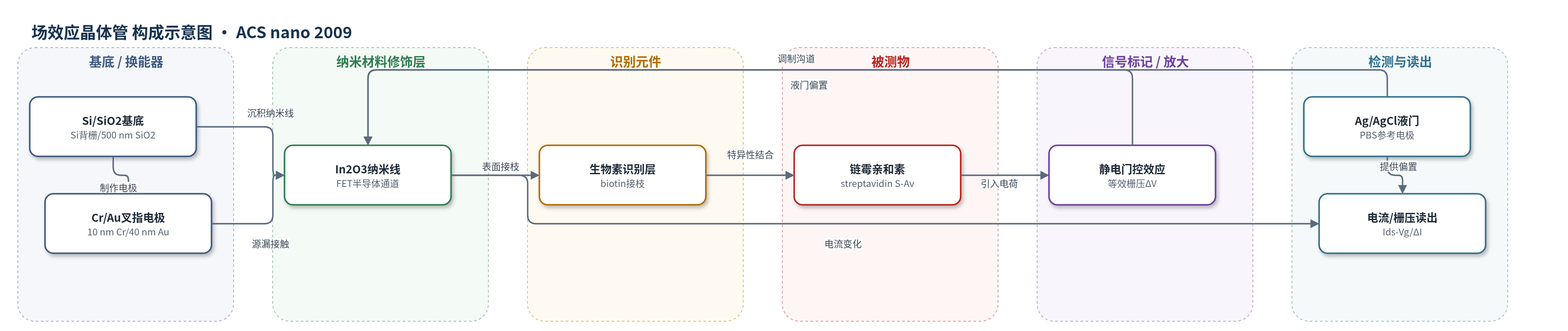
点击图片查看大图 · 依据论文自动绘制
传感器类型
场效应晶体管(FET)生物传感器
检测对象
链霉亲和素(streptavidin, S-Av);样品基质:PBS缓冲液(0.01× PBS等)
检测原理
生物素接枝于In2O3纳米线表面,与溶液中的链霉亲和素特异性结合。链霉亲和素结合口袋附近含氨基,结合后在纳米线表面附近引入正电荷,形成静电门控效应。该静电扰动等效于改变FET栅压,使Ids-Vg曲线发生约14 mV的平行移动,并在固定栅压下产生电流变化ΔI。由于响应随PBS离子浓度/Debye长度变化,说明主要机制是静电相互作用而非电荷转移。校准时将ΔI除以dIds/dVg,可把电流变化转换为等效栅压变化,从而消除阈值电压等器件参数差异。
检测灵敏度
100 nM S-Av 绝对响应: 210、95、35 nA;相关系数: 0.98(ΔI 与 dIds/dVg 线性拟合)
效应效果
器件良率约70%,典型on/off约10^5,70%器件on/off>10^2。校准后CV由59%降至16%(摘要/结论分别报告25%与19%),常规归一化CV为25%;ΔI与dIds/dVg线性相关系数0.98。实时测量等效栅压变化约14 mV。PBS加入无响应,Au标记链霉亲和素SEM证实结合,表明选择性来自生物素-链霉亲和素识别。作者认为该方法可支持大阵列多路生物标志物检测。
传感器的构成
- 基底/栅介质:Si/SiO2(500 nm SiO2)作为背栅与绝缘层,提供FET工作界面
- 源漏电极:10 nm Cr/40 nm Au叉指电极,提供欧姆接触并增大有效沟道宽度
- 换能通道:In2O3纳米线随机分布于源漏电极间,作为半导体通道响应表面电荷变化
- 识别元件:生物素(biotin)接枝于In2O3纳米线表面,特异性结合链霉亲和素
- 液门/参考电极:Ag/AgCl电极浸入PBS缓冲液,作为液门控制界面电势
- 样品池:Teflon池盛装PBS缓冲液,提供离子环境并支持实时加样
- 被测物:链霉亲和素(streptavidin, S-Av)与生物素结合,引入静电扰动
中文摘要
纳米线/纳米管生物传感器因高灵敏度和快速响应而备受关注,但器件间电学参数差异导致定量检测不可靠,是实际应用的主要障碍。本文提出一种基于数据分析的纳米线生物传感器校准方法,以显著抑制传感响应的器件间差异。作者发现生物传感器栅压依赖(dIds/dVg)与绝对响应(电流绝对变化ΔI)之间存在强相关,并以In2O3纳米线FET检测链霉亲和素为模型体系。通过液门效应和不同离子浓度PBS中的响应研究,表明静电相互作用而非电荷转移是主要传感机制。基于该机制和晶体管物理,预测并实验验证ΔI与dIds/dVg呈线性相关。校准方法将每个器件的绝对响应除以dIds/dVg,使不同器件的校准响应趋于一致。与传统按初始电导/电流归一化相比,该方法可消除阈值电压差异带来的影响,显著降低器件间变异,使纳米传感器阵列可用于多路生物分析。
英文摘要
Nanowire/nanotube biosensors have stimulated significant interest; however, the inevitable device-to-device variation in the biosensor performance remains a great challenge. We have developed an analytical method to calibrate nanowire biosensor responses that can suppress the device-to-device variation in sensing response significantly. The method is based on our discovery of a strong correlation between the biosensor gate dependence (dI(ds)/dV(g)) and the absolute response (absolute change in current, DeltaI). In(2)O(3) nanowire-based biosensors for streptavidin detection were used as the model system. Studying the liquid gate effect and ionic concentration dependence of strepavidin sensing indicates that electrostatic interaction is the dominant mechanism for sensing response. Based on this sensing mechanism and transistor physics, a linear correlation between the absolute sensor response (DeltaI) and the gate dependence (dI(ds)/dV(g)) is predicted and confirmed experimentally. Using this correlation, a calibration method was developed where the absolute response is divided by dI(ds)/dV(g) for each device, and the calibrated responses from different devices behaved almost identically. Compared to the common normalization method (normalization of the conductance/resistance/current by the initial value), this calibration method was proven advantageous using a conventional transistor model. The method presented here substantially suppresses device-to-device variation, allowing the use of nanosensors in large arrays.