组成图示
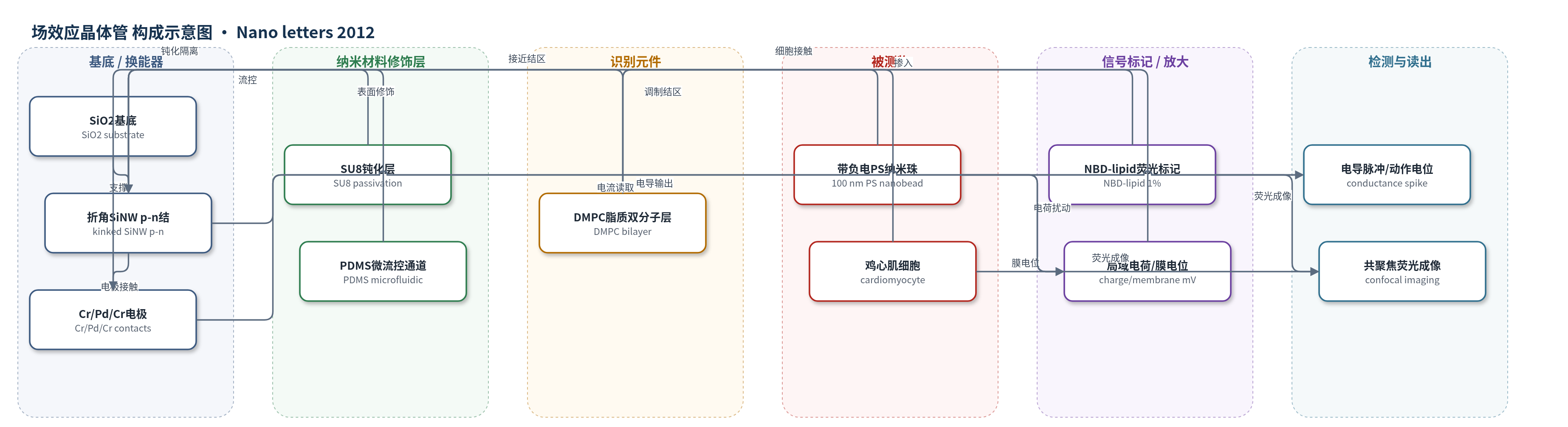
点击图片查看大图 · 依据论文自动绘制
传感器类型
场效应晶体管(FET)生物传感器
检测对象
带负电荷荧光聚苯乙烯纳米珠(charged fluorescent polystyrene nanobeads, PS nanobeads,去离子水/微流控溶液)、鸡心肌细胞动作电位(chicken cardiomyocyte action potentials,Tyrode溶液/活细胞)
检测原理
折角硅纳米线在关节处形成轴向p-n结,p-n结耗尽区暴露于溶液,敏感区局域在折角附近,p型耗尽区半高宽约210 nm。带负电荧光聚苯乙烯纳米珠进入Debye屏蔽长度内或接近p-n结时,其表面负电荷改变结区电势,使p型耗尽区电导增加,产生电导脉冲;纳米珠离开后电导恢复基线。水门实验给出620 nS/V的灵敏度,单珠事件对应约5–6 mV的结电势变化。细胞实验中,DMPC脂质双分子层修饰的三维探针插入鸡心肌细胞,细胞膜电位和动作电位调制p-n结,记录到快速上升>60 mV、200 ms内恢复的胞内动作电位。该传感不依赖酶或核酸放大,而依靠p-n结耗尽区的场效应调制和单颗粒电荷的局域界面效应。
检测灵敏度
灵敏度: 620 nS/V
效应效果
器件在去离子水中对1.2 nM、100 nm带负电荧光聚苯乙烯纳米珠实现单颗粒检测:两独立探针记录非相关on/off脉冲,持续50–200 ms,电导幅度3–4 nS和2–3 nS,校准电势变化5–6 mV;无珠溶液无脉冲。同步共聚焦成像将电导脉冲与单珠接近/扩散关联,并见激光扫描p-n结的光电流峰。3D探针经DMPC双分子层修饰后记录自发跳动鸡心肌细胞,出现约20 mV胞外至胞内静息电位偏移,动作电位快速上升>60 mV、200 ms内恢复,与patch clamp一致;可多次插入/退出同一细胞且细胞存活。作者认为其传感区高度局域,可通过掺杂调节p/n/双极性响应,适用于生物化学传感、纳米光子检测和活细胞/组织三维记录。
传感器的构成
- 基底/换能器:SiO2基底上的折角硅纳米线(SiNW)轴向p-n结,作为局域电荷/电位换能器
- 电极层:Cr/Pd/Cr(1.5/120/60 nm)金属接触,连接p臂与n臂并读取电导
- 钝化层:SU8光刻胶,隔离金属电极与水性介质
- 微流控层:PDMS微流控通道(高50 μm、宽1 mm),引导溶液流过器件
- 生物界面层:DMPC脂质双分子层(1,2-dimyristoyl-sn-glycero-3-phosphocholine),修饰纳米线表面以支持细胞内记录
- 荧光报告层:NBD-lipid(1%掺入DMPC),提供荧光标记以便成像定位
中文摘要
半导体纳米线等半导体纳米材料被广泛研究为场效应晶体管形式的生物/化学传感器,虽在一维和二维器件中表现出高灵敏度,但真正的点状检测器尚未实现。纳米尺度p-n二极管具有吸引力,因为其器件元件天然局域在结附近;尽管纳米线p-n二极管已作为光伏器件被广泛研究,其生物/化学传感应用尚未探索。本文证明p-n二极管器件可作为新型强局域化生物传感器探针。在折角硅纳米线的关节处合成轴向p-n结,扫描电镜证实折角结构,电输运测量显示整流行为和正向偏压下明确的开启。扫描门显微镜表明最敏感区域局域在折角p-n结附近。作者在水溶液中利用带电荷荧光聚苯乙烯纳米珠进行高空间分辨率传感,多路电测量显示明确的单颗粒检测,同步共聚焦成像将纳米珠运动与p-n器件记录的电学信号直接关联。此外,折角p-n结纳米线作为三维探针展示了从电活性细胞记录动作电位的能力。这些器件代表构建纳米探针的新方式,为生物/化学传感、纳米光子检测以及活细胞和组织内的三维记录提供重要机会。
英文摘要
Semiconductor nanowires and other semiconducting nanoscale materials configured as field-effect transistors have been studied extensively as biological/chemical (bio/chem) sensors. These nanomaterials have demonstrated high-sensitivity from one- and two-dimensional sensors, although the realization of the ultimate pointlike detector has not been achieved. In this regard, nanoscale p-n diodes are attractive since the device element is naturally localized near the junction, and while nanowire p-n diodes have been widely studied as photovoltaic devices, their applications as bio/chem sensors have not been explored. Here we demonstrate that p-n diode devices can serve as a new and powerful family of highly localized biosensor probes. Designed nanoscale axial p-n junctions were synthetically introduced at the joints of kinked silicon nanowires. Scanning electron microscopy images showed that the kinked nanowire structures were achieved, and electrical transport measurements exhibited rectifying behavior with well-defined turn-on in forward bias as expected for a p-n diode. In addition, scanning gate microscopy demonstrated that the most sensitive region of these nanowires was localized near the kinked region at the p-n junction. High spatial resolution sensing using these p-n diode probes was carried out in aqueous solution using fluorescent charged polystyrene nanobeads. Multiplexed electrical measurements show well-defined single-nanoparticle detection, and experiments with simultaneous confocal imaging correlate directly the motion of the nanobeads with the electrical signals recorded from the p-n devices. In addition, kinked p-n junction nanowires configured as three-dimensional probes demonstrate the capability of intracellular recording of action potentials from electrogenic cells. These p-n junction kinked nanowire devices, which represent a new way of constructing nanoscale probes with highly localized sensing regions, provide substantial opportunity in areas ranging from bio/chem sensing and nanoscale photon detection to three-dimensional recording from within living cells and tissue.