组成图示
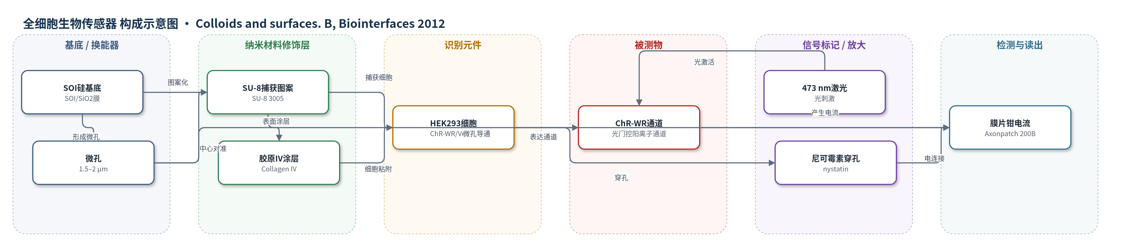
点击图片查看大图 · 依据论文自动绘制
传感器类型
全细胞生物传感器
检测对象
光门控离子通道 ChR-WR(channelrhodopsin wide receiver)的激光诱导通道电流;样品基质:表达 ChR-WR 的 HEK293 细胞全细胞膜片钳体系(bath solution/pipette solution)
检测原理
该传感器以表达ChR-WR的HEK293细胞为识别元件。SU-8细胞捕获图案与胶原IV涂层使细胞稳定覆盖SOI芯片微孔;尼可霉素在细胞膜上形成导电孔,使胞内与pipette solution电连接,构成全细胞膜片钳构型。473 nm激光照射使ChR-WR发生光致构象变化并开放阳离子通道,离子跨膜流动产生膜电流。膜片钳放大器在全细胞模式下记录电流,其幅值随膜电位、通道开放概率和光刺激强度变化,从而反映光门控离子通道功能。系统未使用化学信号放大,主要依靠全细胞多通道开放与低泄漏微孔构型获得可测电流。
检测灵敏度
未报告
效应效果
无细胞捕获图案时,细胞覆盖微孔需数天且易形成多层,通道电流测量成功率约20%;引入SU-8图案后,细胞被捕获并形成覆盖微孔的单层集落,成功率提高至约60%。孵育型构型在约10 kPa负压下获得10–30 MΩ密封电阻,芯片电容约100 pF,尼可霉素穿孔引起约6 pF电容变化。473 nm激光最大输出1.5 mW、光斑10–50 μm,可稳定诱导ChR-WR电流;未转染ChR-WR的HEK293细胞无激光诱导电流,显示选择性。电流波形和I–V特性与吸管膜片钳一致,作者认为该图案可提升孵育型平面膜片钳生物传感器用于离子通道功能分析和高通量筛选的可靠性。
传感器的构成
- 基底/换能器电极:SOI硅基底(Si on insulator, SOI)与1 μm SiO2膜,背面形成1.5–2.0 μm微孔,连接上下腔并作为电生理换能界面
- 微孔保护填充:AZ4903正性光刻胶,临时填充微孔防止SU-8堵塞,之后用丙酮去除
- 细胞捕获图案:SU-8 3005负性光刻胶,形成网格与圆形区域(深约5 μm、宽约4 μm),将细胞限制在微孔周围
- 细胞粘附层:胶原IV(Collagen IV, ECM),涂覆芯片表面,促进HEK293细胞粘附与培养
- 识别元件/传感细胞:表达ChR-WR(channelrhodopsin wide receiver)的HEK293细胞,覆盖微孔形成全细胞构型
- 信号标记物:Venus荧光蛋白标记ChR-WR,用于细胞筛选、定位与观察,不直接产生电信号
- 穿孔电连接试剂:尼可霉素(nystatin,约100 μg/ml),在细胞膜形成导电孔,使胞内与pipette solution电连接
- 读出电极/溶液:AgCl/Ag盐桥电极、bath solution(BS)与pipette solution(PS),提供离子环境并传导膜片钳电流
中文摘要
孵育型平面膜片钳生物传感器中,将传感细胞准确定位在芯片微孔上并在孵育过程中保持原位是关键难题。本文在SOI硅传感器芯片表面制备了由网格和圆形区域组成的细胞捕获图案,圆形区域深约5 μm,中心设有1.5–2.0 μm微孔;芯片表面涂覆细胞外基质胶原IV,并接种表达通道视紫红质宽受体(ChR-WR)的HEK293细胞。无图案芯片上细胞需数天才能覆盖微孔并接近汇合,且易形成多层细胞,导致通道电流无法测量;带图案芯片则能迅速将细胞捕获在圆形区域,经数天孵育形成覆盖微孔的单层细胞集落。采用尼可霉素穿孔形成全细胞构型后,473 nm激光可诱导通道电流,其电流波形和膜电位依赖性与吸管膜片钳测量结果一致。结果表明,细胞捕获图案可显著提高孵育型平面膜片钳生物传感器的测量成功率。
英文摘要
Positioning the sensor cell on the micropore of the sensor chip and keeping it there during incubation are problematic tasks for incubation type planar patch clamp biosensors. To solve these problems, we formed on the Si sensor chip's surface a cell trapping pattern consisting of a lattice pattern with a round area 5 μm deep and with the micropore at the center of the round area. The surface of the sensor chip was coated with extra cellular matrix collagen IV, and HEK293 cells on which a chimera molecule of channel-rhodopsin-wide-receiver (ChR-WR) was expressed, were then seeded. We examined the effects of this cell trapping pattern on the biosensor's operation. In the case of a flat sensor chip without a cell trapping pattern, it took several days before the sensor cell covered the micropore and formed an almost confluent state. As a result, multi-cell layers easily formed and made channel current measurements impossible. On the other hand, the sensor chip with cell trapping pattern easily trapped cells in the round area, and formed the colony consisted of the cell monolayer covering the micropore. A laser (473 nm wavelength) induced channel current was observed from the whole cell arrangement formed using the nystatin perforation technique. The observed channel current characteristics matched measurements made by using a pipette patch clamp.